First, EMI / interference design
EMI is a major challenge for many designers today. Failure to pass the EMI test will result in a significant increase in project costs and a slow schedule, so high-level engineers will look for ways to reduce EMI early in the design process. Because switching regulators with high energy efficiency, so more and more people use, the impact on EMI is also aggravating. A simple way to help suppress the EMI associated with switching power supplies is to use a multiphase spread spectrum clock. Using devices such as the LTC6909 can provide help in at least three ways. First, a silicon oscillator (such as the LTC6909) can be used to set the regulator's switching frequency and ultimately the fundamental EMI frequency out of a sensitive band. Second, the multiple output phases of the LTC6909 can be used to switch different regulators in different phases, thereby reducing the peak switching current that causes EMI. A third improvement provided by products such as the LTC6909 is to spread the switching current in the time domain using spread spectrum modulation (SSFM). This technology does not allow radiation energy to stay long in any receiver's frequency band, thus improving EMI.
Second, low-noise circuit design
Noise is the enemy of a system of high accuracy. At the same time, it is also a topic of great scope. I do not intend to elaborate on this topic here, but rather three examples of noise in electronic circuits and how new products can help minimize these noises. For a complete overview of voltage noise, current noise, resistor noise, and their relationship to amplifier circuits, see Design Note 355 at Linear Technology's website.
1. Amplifier noise in high-speed data conversion circuits
In an analog-to-digital conversion circuit, if you select an ADC with a sufficiently high resolution, quantization noise will no longer be the dominant factor. Designers can therefore divert their attention to other sources of noise, including amplifier noise, voltage reference noise, and clock phase noise, all of which can have an overall system accuracy. When choosing an amplifier, the frequency range is an important factor. Above the corner frequency of 1 / f noise, the broadband voltage noise is measured in nV / √Hz. The wider the bandwidth, the greater the noise, so using a passive or low-noise active filter to filter the signal is an important part of low-noise design. In fact, the amplifier's noise sets the minimum resolution signal, and the distortion determines the maximum signal amplitude that can be accurately measured. Noise and distortion together determine the dynamic range. So, for high-resolution ADC applications, it is important to choose a low-noise and low-distortion ADC driver. An example of such a product is the LTC6409, which has a broadband voltage noise of 1.1nV / √Hz. Coupled with the 88dB spurious free dynamic range SFDR at 100MHz, it offers wide dynamic range drive capability for high speed 14-bit ADCs. For example: When providing a DC coupled single-ended 70MHz drive input to a 14-bit LTC2262-14 at a sampling rate of 150Msps, the resulting SNR and SFDR are 71.1dB and 81.6dB, respectively.
Voltage reference noise
In instrumentation systems, the factors of resolution and accuracy are often the voltage reference stability and noise. Recently, two factors have made voltage reference noise even more important. The first factor is the system power supply voltage is gradually decreasing trend. At lower operating voltages, the noise floor becomes more pronounced. The second factor is that the benchmark stability issue has become less problematic as new benchmarks with high initial accuracy and drift and system designers have been able to more easily calibrate system factors. However, the noise can not be calibrated. To help designers meet the demanding requirements of lower power supply voltage systems, Linear Technology has introduced the LT6655 with unparalleled peak-to-peak noise levels of 0.25ppm. The LT6655 offers seven output voltage options (from 1.25V to 5V) and is an ideal companion chip for high resolution ADCs and DACs required by instrumentation and test equipment. The device's wide operating temperature range and superior stability make it an excellent choice for use in automotive and other harsh environments.
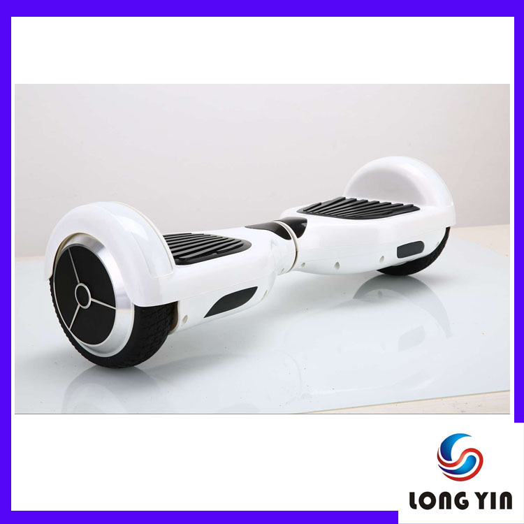
6.5inch Two Wheel Electric Balance Scooter is very hot sales, that motor wheel size is 6.5inch, power total is 500w,use Chinses 36v 4.0Ah lithium battery or Samsung 36v 4.4Ah lithium battery, Max speed is about 10km/h, Range per charge is 15-20Km. Bluetooth, pack bag, remote and top shine lights are option.
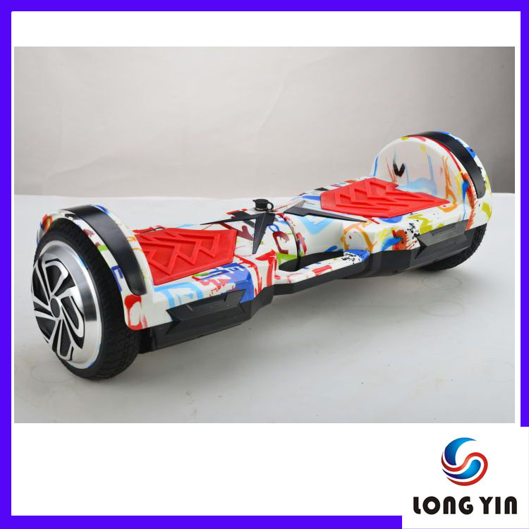
Another 7inch two wheel hoverboard is new production, that is portable. Max load is 120kgs, Min load is 25kgs.Safety climbing angle is about 15 degree. Charger time is 90-120mins.


6.5inch Two Wheel Electric Balance Scooter
6.5Inch Electric Balance Scooter,Wheel Stand Up Electric Scooter,Wheel Electric Scooter,Smart Drifting Scooter
Yongkang Longyin Industry and Trade Co., Ltd. , http://www.cnlongyin.com