[ Instrument R&D of instrumentation network ] Researchers of Eindhoven University of Technology have developed an integrated optical sensor, which is a compact optical sensor that can provide higher resolution and can be applied to lasers and detectors. "Laboratory Chip" platform. Eindhoven University of Technology stated that the new integrated compact sensor is designed for on-chip sensing.
This research is described in Nature Communications.
The developers of Eindhoven said: "Optical readout sensors based on optomechanical systems are often used in sensing applications such as atomic force microscopy to produce sub-nanometer resolution by measuring the laser beam reflected by the deflection of the cantilever. Images. However, traditional laser-based methods (such as those in AFM) may be bulky and accompanied by the need for lower cost and higher resolution, driving people to look for alternative methods.
With the development of nano-optical mechanical systems, compact optical sensors can now be used to measure nano-scale motion, force and mass. But the limiting factor is that the narrow linewidth tunable laser that needs to be applied during the measurement process is difficult to incorporate into this nano-optical mechanical device.
To solve this problem, Liu Tianran, Andrea Fiore and their colleagues at the TU/e ​​Photonic Integration Institute designed a new type of optomechanical device with a resolution of 45 femtometres (45×10-15) m), the measurement time is only a few minutes. one second. The developer added: "It is essential that the device has an ultra-wide optical bandwidth of 80 nm, thereby directly eliminating the need for tunable lasers."
Waveguide and large wavelength range
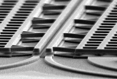
The sensor is based on an indium phosphide silicon film platform and is suitable for including passive components such as lasers or detectors. The sensor itself consists of four waveguides-two waveguides are suspended above the two output waveguides.
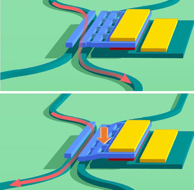
Light passing through the directional coupler before (upward) and after (downward) driving.
When the suspended waveguide is pushed to the output waveguide on the InP film, the relative signal quantity carried by the output waveguide will change.
The manufacturing process defines the waveguide and cantilever through a series of lithography steps. The final sensor consists of a transducer, actuator, and photodiode.
One of the main advantages of this sensor is that it can work in a large wavelength range, thereby eliminating the need for expensive lasers on the device. In terms of cantilever deflection, the sensor also replicates the resolution of the cantilever in traditional but bulky AFM.
The researchers said that based on this new device, they “plan to develop an entire nanometering laboratory integrated on the chip that can be used for semiconductor metrology and help design the next generation of microchips and nanoelectronic products.
Server Chassis Mould Paint,Server Chassis Mould Steel,Server Chassis Mould Unit,Server Chassis Moulding
Kunshan Wangdaxin Precision Mould Co., Ltd. , https://www.wdxmould.com